The technology
Learn about the Timepix chip
and its applications.
Introduction
The Timepix chip is a silicon chip developed at CERN in the framework of the CERN Medipix2 Collaboration. The chip is divided into a 256×256 grid of tiny pixels, similar to the pixels of a phone camera. However, unlike camera pixels, each one contains thousands of transistors that allow it to detect and analyse radiation.
If the chip is combined with a semiconductor sensor, the resulting detector can measure radiation. When a particle passes through the sensor, it deposits energy, creating signals in individual pixels. From these signals, its energy, timing, and spatial pattern can be measured, allowing to identify its type.
Technical details
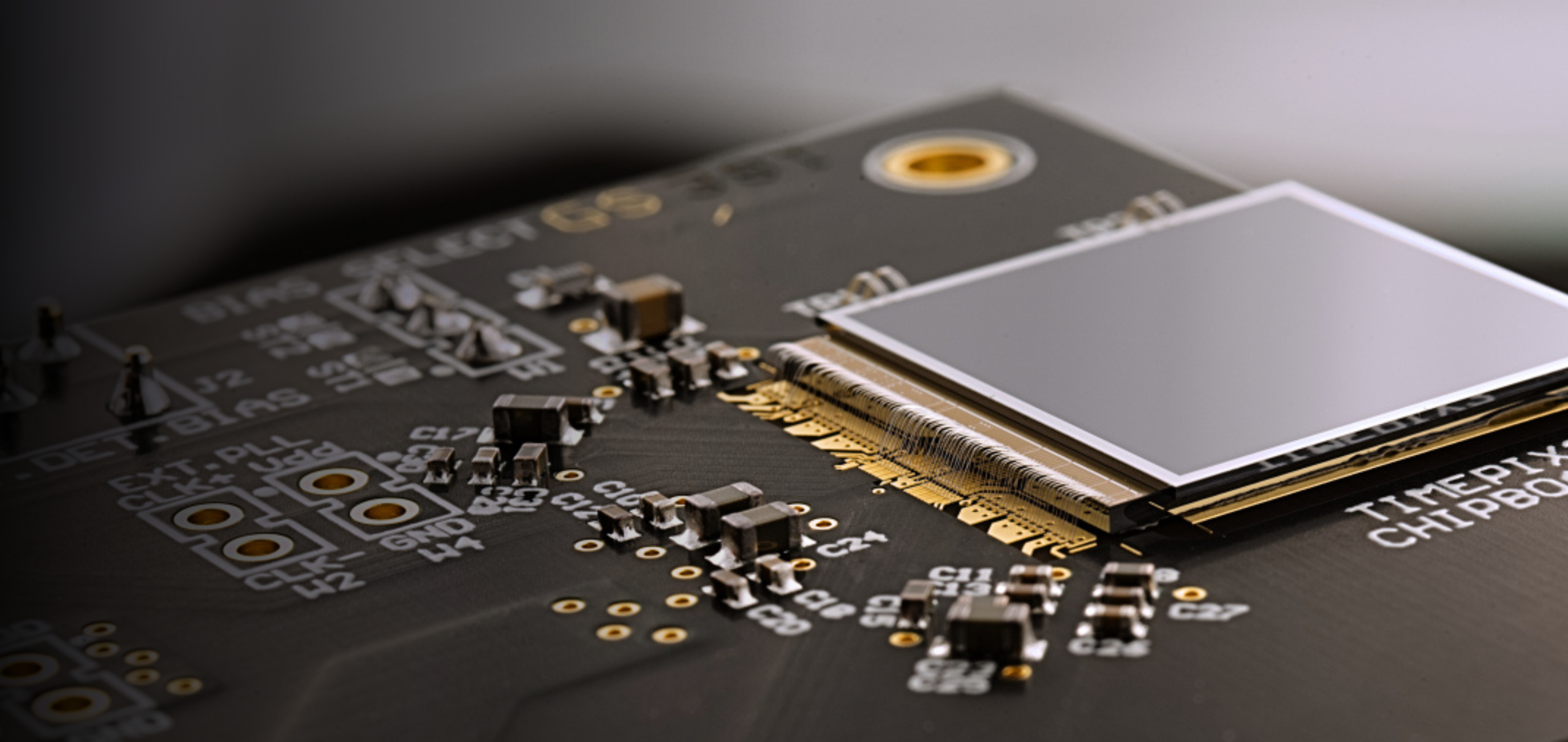
The Timepix chip consists of a pixelated electronics layer Timepix ASIC (Application-Specific Integrated Circuit) readout chip. The detector is a 256×256 matrix of pixels (55µm square) and each of the 65 thousand pixels is a detecting element with a complete electronic signal processing chain, comprising of a preamplifier, a discriminator and a counter.
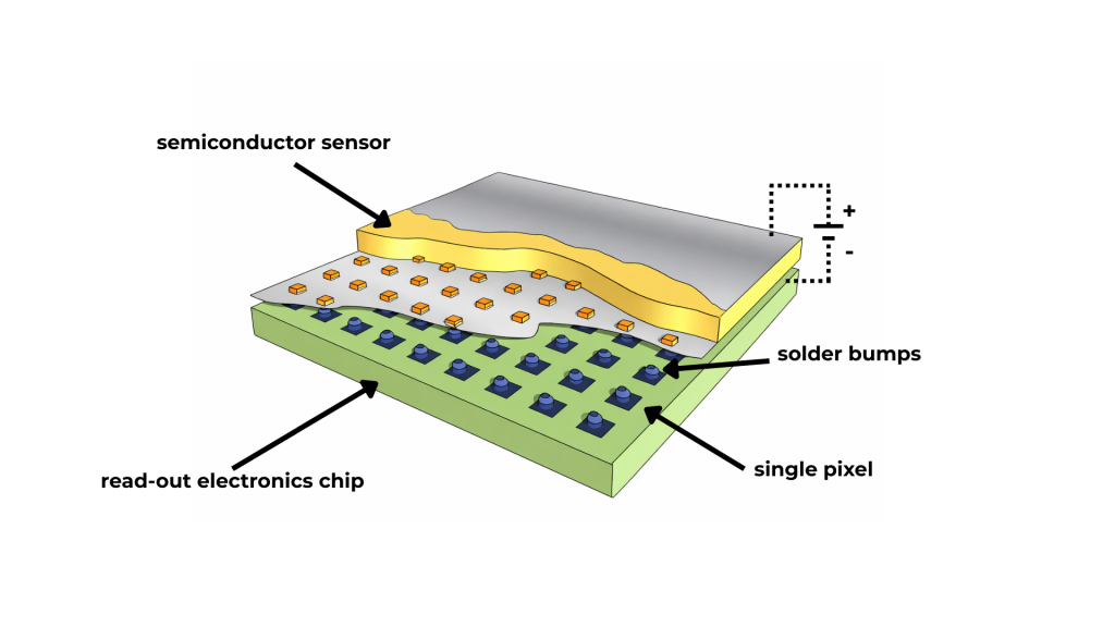
The chip, when combined with semiconductor sensors, provides real-time images of ionising radiation. An ionising particle generates thousands of free electrons as it interacts with the semiconductor silicon sensor. These charges move in the applied electric field inducing a current at the input of the corresponding amplifier connection. The electronics in each pixel can measure the amplitude of this signal. When properly calibrated, the detector permits the measurement of the particle’s energy deposition in the pixel.
The Timepix detector belongs to the family of hybrid pixel detectors. The term “hybrid” stems from the fact that the two main elements from which these devices are built, the semiconductor sensor and the pixelated readout chip, are manufactured independently and later electrically coupled by means of a bump-bonding process. This physical separation between the sensor and the readout electronics allows to optimize the choice of the sensor material depending on the application. For example, in High Energy Physics, hybrid pixel detector readout chips are used with silicon as sensor material because of its low mass, its homogeneity and low cost. Other applications, for example X-ray radiography, use high Z sensor materials like Gallium Arsenide (GaAs) and Cadmium Telluride (CdTe).
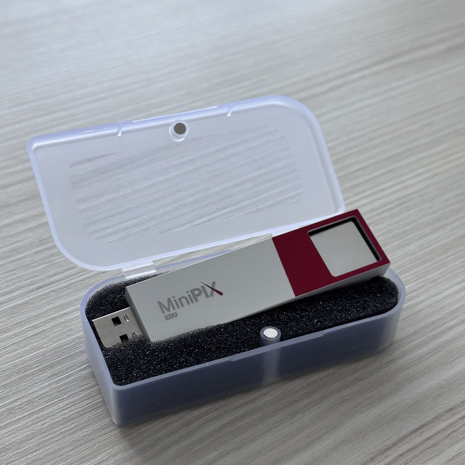
MiniPIX EDU
The MiniPIX EDU detector is a compact, low-power radiation detector based on a single Timepix detector (256 x 256 pixels with a pitch of 55 μm) with 300 or 500 μm thick silicon.
It is manufactured and distributed by ADVACAM, a spin-off company originating from the Medipix Collaborations, specialising in pixel detector technology and radiation imaging solutions.
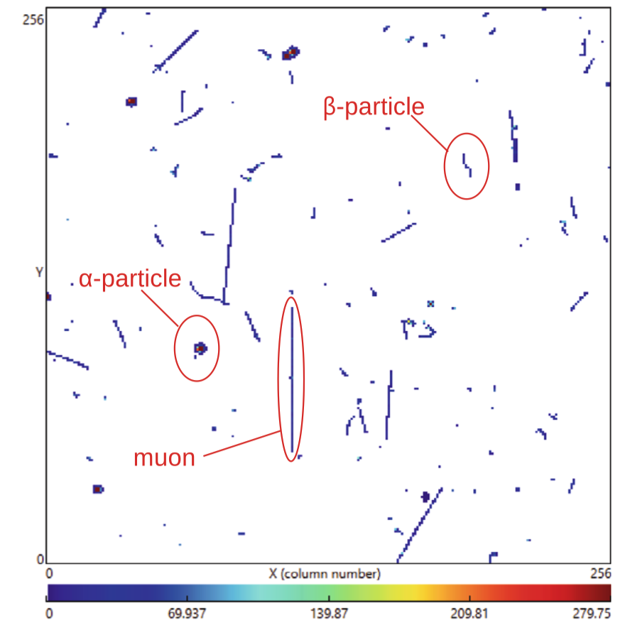
The device connects to a computer via USB and works with user-friendly software, making it easy to integrate into classroom experiments. With the software, students can visualise individual particles, such as alpha, beta, gamma, and cosmic radiation. Thanks to the detector’s high pixel segmentation, looking at the shape of the clusters on a computer screen, one can distinguish heavy-charged particles (thick tracks) from light-charged particles (thin tracks), low-energy photons (typically one or 2-pixel clusters), alphas (blobs), and beta particles (worm-like tracks), as all these interact different with the sensor material.
Applications
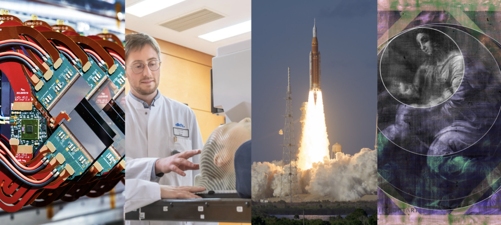
It is very inspiring for students to know that the detectors that are holding in their hands were originally developed at CERN, and find applications in high-energy physics, space, medicine, and art.
To learn more about real-world applications of the Timepix devices, visit the Medipix website.
History of the Medipix collaborations
The Medipix Collaboration was born in the 90’s to bring the technology of the pixel detectors used at LHC experiments to medical applications. Since the first Medipix1 chip, providing noise-free, single-photon counting technology, a family of Medipix technologies has emerged. The Medipix2 chip includes improved spatial resolution; Timepix, a modified version of Medipix2, enables time or amplitude measurements; Medipix3 and Timepix3 extend the functionality by determining the energy level of each individual photon detected. The Collaboration continues to evolve, with its most recent developments being the Medipix4 and Timepix4 ASICs.
The industrial partners and licence holders commercialising the Medipix technology range from established enterprises to young start-up companies, and from applications within medical imaging to education, space dosimetry, and material analysis.
You can learn about the history of the Medipix Collaborations in the video below.